
| Part Number | MC88913 |
| Manufacturer | Motorola |
| Title | LOW SKEW CMOS CLOCK DRIVER |
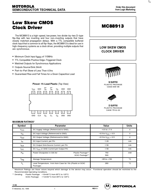
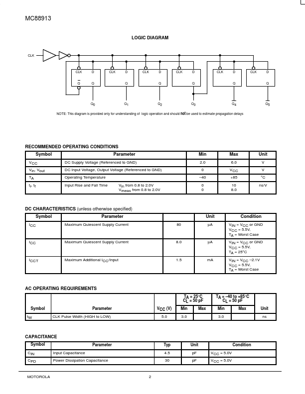
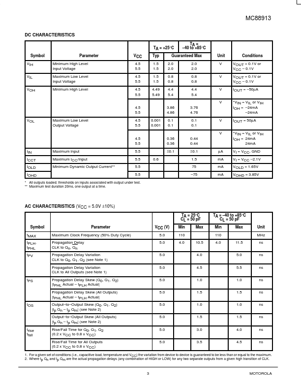
| Description | MOTOROLA SEMICONDUCTOR TECHNICAL DATA Order this document from Logic Marketing Low Skew CMOS Clock Driver The MC88913 is a high–speed, low powe... |
| Features |
* Symbol
VCC Vin Vout Iin Iout ICC PD Tstg TL
Parameter
DC Supply Voltage (Referenced to GND) DC Input Voltage (Referenced to GND) DC Output Voltage (Referenced to GND) DC Input Current, per Pin DC Output Sink/Source Current, per Pin DC VCC or GND Current per Output Pin Power Dissipation in Still A... |
| Published | Apr 30, 2005 |
| Datasheet |
|
| Part Number | MC88916DW |
| Manufacturer | Motorola |
| Title | LOW SKEW CMOS PLL CLOCK DRIVER WITH PROCESSOR RESET |
| Description | of the RST_IN/RST_OUT(LOCK) Functionality The RST_IN and RST_OUT(LOCK) pins provide a 68030/040 processor reset function, with the RST_OUT pin als. |
| Features |
<1ns Skew Each Being Phase and Frequency Locked to the SYNC Input • The Phase Variation From Part –to –Part Between SYNC and the ‘Q’ Outputs Is Less Than 600ps (Derived From the TPD Specification, Which Defines the Part –to –Part Skew) 20 1 • SYNC Input Frequency Range From 5MHZ to 2X_Q FMax/4 • Addit. |
| Datasheet |
|


| Part Number | MC88916 |
| Manufacturer | Motorola |
| Title | LOW SKEW CMOS PLL CLOCK DRIVER WITH PROCESSOR RESET |
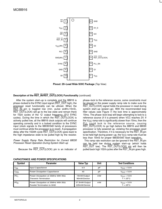
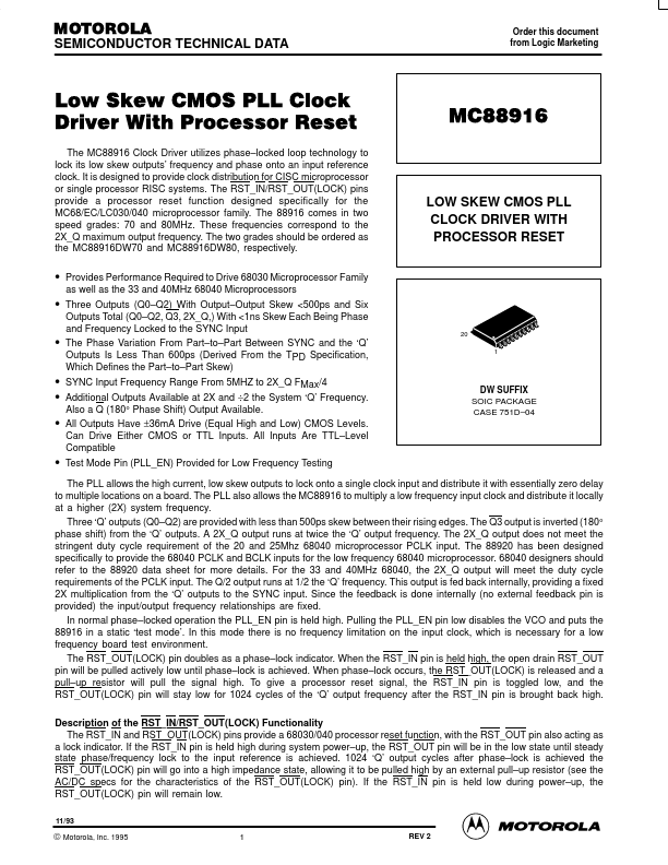
| Description | of the RST_IN/RST_OUT(LOCK) Functionality The RST_IN and RST_OUT(LOCK) pins provide a 68030/040 processor reset function, with the RST_OUT pin als. |
| Features |
<1ns Skew Each Being Phase and Frequency Locked to the SYNC Input • The Phase Variation From Part –to –Part Between SYNC and the ‘Q’ Outputs Is Less Than 600ps (Derived From the TPD Specification, Which Defines the Part –to –Part Skew) 20 1 • SYNC Input Frequency Range From 5MHZ to 2X_Q FMax/4 • Addit. |
| Datasheet |
|

| Part Number | MC88915TFN70 |
| Manufacturer | Motorola |
| Title | LOW SKEW CMOS PLL CLOCK DRIVER |
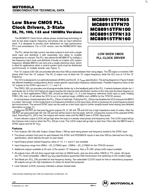
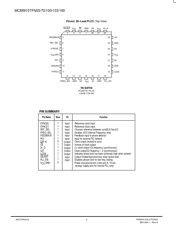
| Description | on page 11). Pulling the OE/RST pin low puts the clock outputs 2X_Q, Q0–Q4, Q5 and Q/2 into a high impedance state (3–state). After the OE/RST pin. |
| Features |
• Five Outputs (Q0 –Q4) with Output –Output Skew < 500 ps each being phase and frequency locked to the SYNC input • The phase variation from part –to –part between the SYNC and FEEDBACK inputs is less than 550 ps (derived from the tPD specification, which defines the part –to –part skew) • Input/Output p. |
| Datasheet |
|


| Part Number | MC88915TFN55 |
| Manufacturer | Motorola |
| Title | LOW SKEW CMOS PLL CLOCK DRIVER |
| Description | on page 11). Pulling the OE/RST pin low puts the clock outputs 2X_Q, Q0–Q4, Q5 and Q/2 into a high impedance state (3–state). After the OE/RST pin. |
| Features |
• Five Outputs (Q0 –Q4) with Output –Output Skew < 500 ps each being phase and frequency locked to the SYNC input • The phase variation from part –to –part between the SYNC and FEEDBACK inputs is less than 550 ps (derived from the tPD specification, which defines the part –to –part skew) • Input/Output p. |
| Datasheet |
|

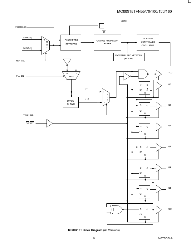
| Part Number | MC88915TFN160 |
| Manufacturer | Motorola |
| Title | LOW SKEW CMOS PLL CLOCK DRIVER |
| Description | on page 11). Pulling the OE/RST pin low puts the clock outputs 2X_Q, Q0–Q4, Q5 and Q/2 into a high impedance state (3–state). After the OE/RST pin. |
| Features |
• Five Outputs (Q0 –Q4) with Output –Output Skew < 500 ps each being phase and frequency locked to the SYNC input • The phase variation from part –to –part between the SYNC and FEEDBACK inputs is less than 550 ps (derived from the tPD specification, which defines the part –to –part skew) • Input/Output p. |
| Datasheet |
|
